RSL10 Hackery
Overview
The On Semiconductor RSL10 System on a Chip (SoC) is a really neat, very low power microprocessor / RF front end combination chip. The objective of this rough page is to outline the process of getting started developing applications with the On Semiconductor RSL10 SDK and dive deeper into some of the functionalities of this chip.
Table of Contents
- Getting to Blinky
- Figuring Out How to View printfs
-
Using the ADC
Getting to Blinky
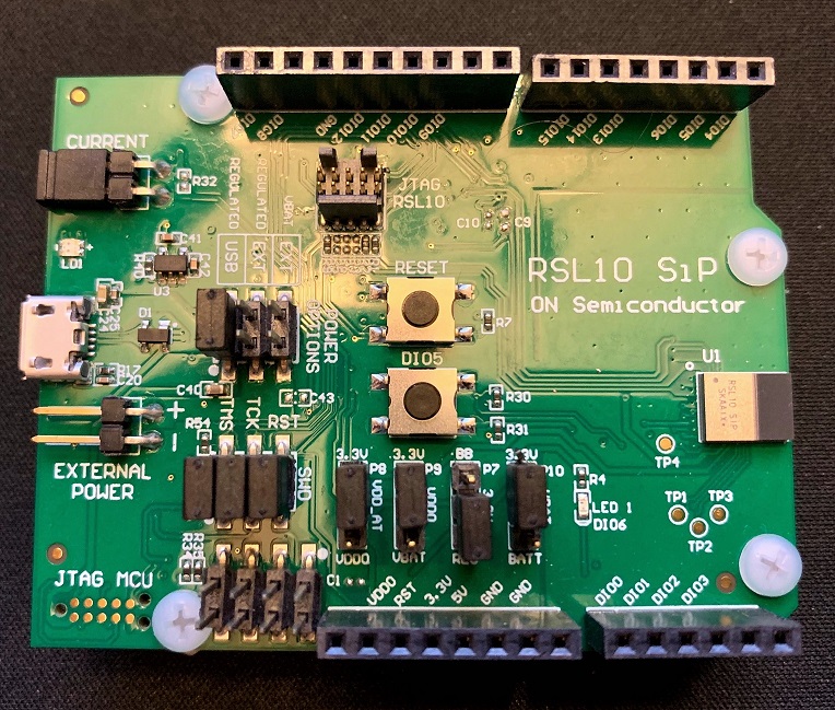
Fortunately, the getting started PDF straight from On Semi was actually extremely comprehensive and provided pretty much step by step instructions from unboxing the SoC development board, to installing the Eclipse based SDK, to loading the blinky example code, to finally programming the SoC board and running the blinky code on the platform. All in all, the process of unboxing the SoC to running the blinky example took less than an hour and a half. You can find this excellent piece of documentation here.
Figuring out how to view printfs
Print Configuration out of the Box
The print.h file which the Blinky example includes looks like this out of the box from the SDK
#ifndef PRINTF_H
#define PRINTF_H

#define OUTPUT_DISABLED                -1
#define OUTPUT_UART                    0 /* Note: if application uses UART or DIO5, PRINTF over UART will be a conflict.  */
#define OUTPUT_RTT                     1 /* Note: for RTT PRINTF, add the SEGGER RTT component on your .rteconfig file */

 #ifndef OUTPUT_INTERFACE
     #define OUTPUT_INTERFACE           OUTPUT_DISABLED
 #endif

#if OUTPUT_INTERFACE == OUTPUT_UART
    #define THREE_BLOCK_APPN(x, y, z)       x##y##z
    #define DMA_IRQn(x)                     THREE_BLOCK_APPN(DMA, x, _IRQn)
    #define DMA_IRQ_FUNC(x)                 THREE_BLOCK_APPN(DMA, x, _IRQHandler)
    #define VA_NARGS_IMPL(_1, _2, _3, _4, _5, _6, _7, _8, _9, _10, _11, _12, _13, _14, _15, _16, _17, _18, _19, _20, N, ...) N
    #define VA_NARGS(...) VA_NARGS_IMPL(__VA_ARGS__, 20, 19, 18, 17, 16, 15, 14, 13, 12, 11, 10, 9, 8, 7, 6, 5, 4, 3, 2, 1)
    int UART_printf(const int narg, const char *sFormat, ...);
    #define PRINTF(...) UART_printf(VA_NARGS(__VA_ARGS__), __VA_ARGS__)
    void printf_init(void);
    void DMA_IRQ_FUNC(DMA_UART_TX)(void);

#elif OUTPUT_INTERFACE == OUTPUT_RTT
#include <SEGGER_RTT.h>
    void printf_init(void);
    #define PRINTF(...) SEGGER_RTT_printf(0, __VA_ARGS__)
#else
    #define PRINTF(...)
    #define printf_init()
#endif

#endif /* PRINTF_H */
Custom Print Configuration
You’ll notice in the code snippet above that the printf statements are disabled by default but we are given two options for outputting print statements: RTT and UART. I found the documentation (linked above) to be perhaps out of date with the SDK code examples for this particular development board. Part of the confusion with getting print statements to work revolved around just how the development board was being programmed over USB and whether we needed to utilize RTT or UART. Long story short, I found that by switching:
 #ifndef OUTPUT_INTERFACE
     #define OUTPUT_INTERFACE           OUTPUT_DISABLED
 #endif
to
  #ifndef OUTPUT_INTERFACE
     #define OUTPUT_INTERFACE           OUTPUT_UART
 #endif
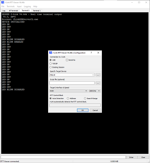
Got print statements working. One final gotya though : In order to actually see the print statements in realtime, you need to use the J-Link Viewer application (which the SDK installs during the J-Link driver install process).
Using the J-Link Viewer
Fortunately viewing the UART output of the RSL10 via the J-Link programmer built into the on-board ARM Cortex chip, is super easy. Once you launch the J-Link Viewer application, simply configure the settings as they are in the following picture, click the “go” button, and switch to the “All Terminals” tab.
Using the ADC
The RSL10 SDK ships with an ADC example which implements all the necessary code to read from one of the system’s specific analog-to-digital converters (ADC) which happens to be connected to the battery voltage input line. This particular example, called “ADC_UART”, reads from this specific Battery Monitor ADC, adds 100 battery voltage samples to a summation variable, and then divides that variable by 100 to end up with an average battery voltage sample. Simple enough, right?
 /* Disable all existing interrupts, clearing all pending source */
    Sys_NVIC_DisableAllInt();
    Sys_NVIC_ClearAllPendingInt();

    /* Test DIO12 to pause the program to make it easy to re-flash */
    DIO->CFG[RECOVERY_DIO] = DIO_MODE_INPUT  | DIO_WEAK_PULL_UP |
                             DIO_LPF_DISABLE | DIO_6X_DRIVE;
    while (DIO_DATA->ALIAS[RECOVERY_DIO] == 0);

    /* Prepare the 48 MHz crystal
     * Start and configure VDDRF */
    ACS_VDDRF_CTRL->ENABLE_ALIAS = VDDRF_ENABLE_BITBAND;
    ACS_VDDRF_CTRL->CLAMP_ALIAS  = VDDRF_DISABLE_HIZ_BITBAND;

    /* Wait until VDDRF supply has powered up */
    while (ACS_VDDRF_CTRL->READY_ALIAS != VDDRF_READY_BITBAND);

    /* Enable RF power switches */
    SYSCTRL_RF_POWER_CFG->RF_POWER_ALIAS   = RF_POWER_ENABLE_BITBAND;

    /* Remove RF isolation */
    SYSCTRL_RF_ACCESS_CFG->RF_ACCESS_ALIAS = RF_ACCESS_ENABLE_BITBAND;

    /* Start the 48 MHz oscillator without changing the other register bits */
    RF->XTAL_CTRL = ((RF->XTAL_CTRL & ~XTAL_CTRL_DISABLE_OSCILLATOR) |
                     XTAL_CTRL_REG_VALUE_SEL_INTERNAL);

    /* Enable 48 MHz oscillator divider to generate an 8 MHz clock. */
    RF_REG2F->CK_DIV_1_6_CK_DIV_1_6_BYTE = CK_DIV_1_6_PRESCALE_6_BYTE;

    /* Wait until 48 MHz oscillator is started */
    while (RF_REG39->ANALOG_INFO_CLK_DIG_READY_ALIAS !=
           ANALOG_INFO_CLK_DIG_READY_BITBAND);

    /* Switch to (divided 48 MHz) oscillator clock */
    Sys_Clocks_SystemClkConfig(JTCK_PRESCALE_1 |
                               EXTCLK_PRESCALE_1 |
                               SYSCLK_CLKSRC_RFCLK);

    /* Setup DIO6 as a GPIO output */
    Sys_DIO_Config(LED_DIO, DIO_MODE_GPIO_OUT_0);

    /* Initialize the UART and associated DMA */
    UART_Initialize();

    /* Set the ADC configuration */
    Sys_ADC_Set_Config(ADC_VBAT_DIV2_NORMAL | ADC_NORMAL | ADC_PRESCALE_1280H);

    /* Set the battery monitor interrupt configuration */
    Sys_ADC_Set_BATMONIntConfig(INT_EBL_ADC |
                                ADC_CHANNEL <<
                                ADC_BATMON_INT_ENABLE_ADC_INT_CH_NUM_Pos |
                                INT_EBL_BATMON_ALARM);

    /* Set the battery monitor configuration, use channel ADC_CHANNEL to battery
     * monitoring. */
    Sys_ADC_Set_BATMONConfig((100 << ADC_BATMON_CFG_ALARM_COUNT_VALUE_Pos) |
                             (THRESHOLD_CFG <<
                              ADC_BATMON_CFG_SUPPLY_THRESHOLD_Pos) |
                             BATMON_CH(ADC_CHANNEL));

    /* Configure ADC_CHANNEL input selection to VBAT/2 */
    Sys_ADC_InputSelectConfig(ADC_CHANNEL, ADC_POS_INPUT_VBAT_DIV2 |
                              ADC_NEG_INPUT_GND);

    /* Configure both input selection for an ADC channel to GND so the OFFSET is
     * subtracted automatically to result. */
    Sys_ADC_InputSelectConfig(ADC_GND_CHANNEL, ADC_POS_INPUT_GND |
                              ADC_NEG_INPUT_GND);

    /* Enable interrupts */
    NVIC_EnableIRQ(ADC_BATMON_IRQn);
Well in theory,
yes
, simple. In practice (as you see above), this example requires a 8MHz clock signal to trigger a function which samples from the ADC 8 million times a second. This dedicated sampling function is configured as an interrupt and linked to the 8Mhz clock trigger when everything is configured initially.
All of this ends up leading to (in my opinion) a fair bit of opaque configuration code which makes me want to bang my head against a wall. So, what we’ll walk through now is how to sample with an ADC of our choosing by manually asking for the current measurement instead of automatically scheduling an interrupt to do so for us.